Trying not to mar flap cross tube too bad with Upstops 5 of 7
Date: 12/26/2013
Views: 5957
13062003173338_G
Date: 12/31/1969
Views: 2535
Newest Image
EAA SITE
Date: 08/23/2023
Views: 191388
Tri State Logic help needed 2.
Hi Ron,
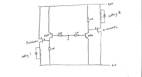
On the Tri-state logic.Attached a sketch using 4 transistors, 4 resistors and 2 relays with diodes.
It works as follows:
A
point S not connectedS is at about 1/2 battery voltagePNP and NPN transistor both fully conductingVgs for both N-channel FET and P-channel FET are zeroBoth FETs not conducting, relays nor energized
B
point S connected to battery voltageNPN transistor and N-channel FET same as APNP transistor now not conducting and Vgs of P-channel FET is negativebattery voltageP-channel FET fully conducting and relay 1 energized C
point S connected to groundPNP transistor and P-channel FET same as ANPN transistor now not conducting and Vgs of N-channel FET is positivebattery voltageN-channel FET fully conducting and relay 2 energized Concerning S voltage: there is a large band, from 0.6 V above ground to0.6 V below battery voltage where neither relay is energized.Only a hard connection to a rail (ground or battery) energizes one orthe other relay. If you are interested in this solution I have some more remarks to makeand I can give you Digikey or Mouser part numbers.
Hi Ron, Absolutely right. 10V or so zeners are required between gate and source of the FETs.I think picking 300V transistors and >70V or so FETs makes it then safe enough for DO-160 compliance.There is one more thing.As drawn with steady power there is no chance for both relays to be energized at the same time.
A possible concern though is power up / power down. On power up there is a theoretical possibility that Vgs of a FET will not be clamped down in time on startup.The best way to preclude that is to also put a capacitor of between 1nF and 10nF or so between gate and source of the FETs, making them slower in a controlled way.For the relays the switching speed makes no difference (they are a 1000 times slower still), for the FETs (they will dissipate more energy during a transition) it also makes no difference because the transition duty cycle is so low (less than 1/1000).Power down not a problem I believe.I would still like to test with an oscilloscope though. How to make.What I do with these 1-off simple circuits is the following:
1. I have double or single sided copper clad good quality fiberglass-epoxy board
2. I have a small handful of smd parts
3. I have a schematic
4. I design where all the parts will go on the boards and the cuts to be made in the copper layer
5. Leaving large pads on the periphery for soldering leads to the outside world
6. I make the cuts using a dremel witha. cutting wheelb. small circular sawc. small routing bit
7. I solder the smd pieces on
8. Soldering smds requires some tools and a bit of exercise:"Surface Mount Soldering Tutorials" at http://www.sparkfun.com/commerce/tutorials.php Alternatively you can use through hole parts on a perforated board.Holes at 0.1" spacing, row holes connected with copper cladding on the back, columns not connected.You cut copper rows where required and connect different rows with wire where required.I find the result generally less satisfying for reasons of robustness and bulk, but it is easier to do. Having thought about the problem and wanting to check out the solution I wouldn't mind making two boards for you if you would lend your address as a conduit for some of the required parts (all kinds of expenses if I would order directly to my address in NL).
Hi Jan> > Wayne e-mailed me back:> "I like Jan's idea, I would just ask if he'd recommend zeners on the > FET gates to limit voltage. The part numbers would save time too, tell > him thanks."
Y10-06-01


